Why 100G Data Center Transceiver Prefers COB Packaging?
Jul. 14, 2021
Depending on the application environment, optical modules can be divided into data center grade and telecom grade. The telecom market is harsh and demanding, requiring high reliability and low cost for optical modules; data center grade optical modules have lower performance requirements than telecom grade, such as temperature requirements, but also feature high rate requirements, rapid iteration and high demand, requiring packaging processes that are more suitable for data center market demand. The next 100G optical module supplier will explain why COB packaging process is more suitable for data center 100G optical module.
Common Optical Module Packaging Processes
The basic structure of optical module packaging is the transmitter side module (TOSA) and driver circuit, the receiver side module (ROSA) and receiver circuit, in which the process of packaging lasers and detectors into TOSA and ROSA is the core of optical module packaging and the main technical barrier. package, BOX package, and FlipClip, etc.
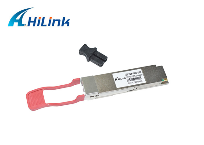
COB package is chip-on-board package, the laser chip is directly adhered to the PCB, saving PCB area, and also improving performance because of building a shorter interconnection path, for 100G QSFP28 optical module COB package is more suitable.

Why COB packaging process is more suitable for data centre 100G optical modules?
1. Save volume and meet high density requirements. Traditional single-way 10Gb/s or 25Gb/s rate optical modules use SFP package to weld the electrical chip and TO package optical transceiver components to the PCB board to form an optical module. While the 100Gb/s optical module, in the use of 25Gb/s chip, requires four groups of components, if the SFP package, will require four times space.COB package can be TIA / LA chip, laser array and receiver array integrated package in a small space to achieve miniaturization.
2. The process itself is suitable for mass production to meet the requirements of high demand and low cost.COB package adheres the laser chip directly to the PCB, eliminating the complex packaging steps, which can reduce the production cost, and with the maturity of related technology and equipment operation, mass production becomes simpler, compared to TO-CAN package and BOX package which rely more on manual power.
3.Compared with other packages, the advantages are outstanding. TO-CAN package is more suitable for low-rate optical modules, with mature process and high yield, but less suitable for mass production; butterfly package is costly, more suitable for lasers and higher reliability requirements of the field, such as telecommunications-grade optical modules.
It should be noted that the COB package is still technically difficult for the precise positioning of the chip to fit, and the yield of the optical module is not optimal, so special attention should be paid to the performance testing of the optical module.
Conclusion
On the whole, COB package meets the requirements of high reliability and low cost, and is the mainstream package type for 100G QSFP28 optical module. In the face of the product yield problem, FMS(FS) has strictly controlled the quality of 100G QSFP28 optical module products after multiple optical and compatibility testing processes to guarantee the qualification rate of optical modules.


